
Laser direct structuring (LDS) is a special success story. It has been possible to apply electronic conductor tracks directly to plastic parts in series production for almost 20 years. LDS enables the production of electronic assemblies with flexible geometric shapes. This process allows electronic products (such as smart phones, sensors or medical equipment) to become even smaller and more powerful. Automated manufacturing processes also make this process more economically attractive.
With less and less space available for electronic assemblies, solutions are needed that replace conventional printed circuits. LDS enables further miniaturization and increasingly complex geometric designs. It is a stable and reliable process that has proven itself in quality-critical sectors such as medical technology or safety-relevant components for the automotive industry.
The LDS process enables three-dimensional assemblies
Direct laser structuring enables the production of 3D-MID (Mechatronic Integrated Devices) assemblies. 3D-MID allows electronic components to be mounted directly on a three-dimensional base body, without printed circuit boards or connecting cables. The basic housing is manufactured using an injection molding process, in which a non-conductive, inorganic additive is added to the thermoplastic material.
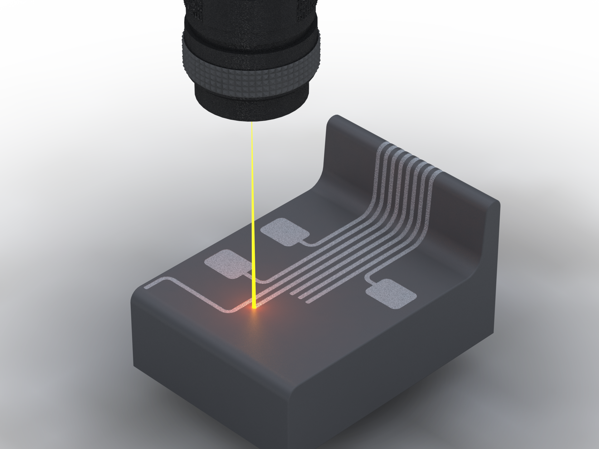 Laser Direct Structuring (LDS)
The structure of the conductor track is applied using the LDS process.
LDS makes it possible to create electronic assemblies in flexible geometric shapes. Smart phones, hearing aids and smart watches become smaller and more powerful thanks to this process.
The additives in the material are “activated” by direct laser structuring, allowing the plastic material to contain the electrical conductor paths. The laser beam describes the areas intended for the conductor paths and creates a micro-rough structure. The released metal particles form the nuclei for the subsequent chemical metallization. In this way, the electrical conductor paths are applied to the areas marked by the laser. The other parts of the three-dimensional basic body remain unchanged. The plastic component can then be assembled in standard SMD processes, similar to a conventional PCB. It is also suitable for soldering in a reflow oven.
Versatile application of laser technology
HARTING 3D-MID AG is the largest supplier of 3D-MID components outside Asia. HARTING uses high-quality laser systems for the LDS process, with three lasers working in parallel, each rotated by 45 degrees. Thanks to an additional rotation axis, components can be processed simultaneously by the laser from all sides (360 degrees). This technology makes it possible to create flexible geometric shapes, such as reflector shells or LED lamps. Despite the minimum thickness of the conductor paths of 16 to 20 μm, the conductor paths are still suitable for demanding automotive parts or for applications with currents up to 10 A – for example for heating coils in cameras that are used to prevent the optics from fogging.
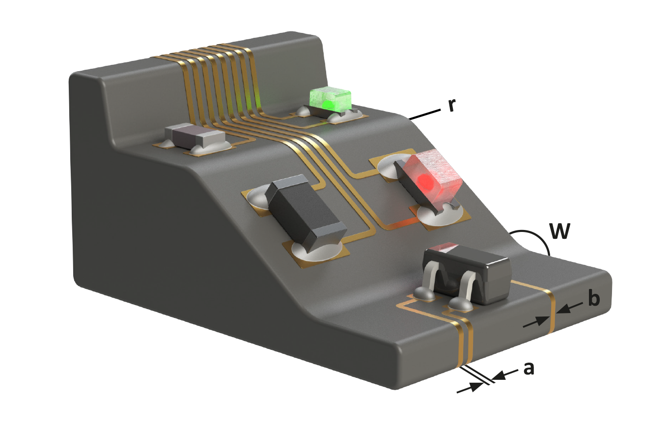 Dimensioning and positioning
Minimum distances between conductor paths (a): 50 – 150 μm. Minimum width of the conductor paths (b): 50 – 150 μm
Radius (r): 0.2mm
Frequent changes during the electronics development phase or new components with changed dimensions can lead to expensive adjustments during conventional printed circuit board production. The laser layout, on the other hand, can be adjusted very flexibly by using the parameters of the laser's control software. This does not require any adjustments to the injection molding.
Prototype production with LDS is also easier compared to conventional processes. HARTING can produce the plastic base body using LDS compatible material and 3D printing. Injection molding can also be used with inexpensive prototyping tools.
New trends in the LDS process
Several aspects of LDS technology have been improved and developed in recent years.
- The working area of the laser has been increased from 160 x 160 x 80 mm to 200 mm x 200 mm x 80 mm, allowing higher packing density and the processing of even larger components.
- The working speed of the laser can be doubled to 4 m/s by optimizing the servo units and the mirrors that guide the laser beam, significantly reducing the machining time.
- The improvement in optics allows the use of a laser with a diameter of 100 μm and a laser with a fine focus of 50 μm for the processing of even smaller structures.
HARTING is the only one 3D MID manufacturer in the world that has a laser system with three fine focus optics of 50 μm. Thanks to this fine-focus laser, even smaller guide paths can be realized. This allows many conductor paths to be created on the same component and a higher packing density can be achieved. This is used, among other things, for safety technology, because the closely spaced and intertwined conductors are able to activate safety alarms in the event of even the slightest physical interference.
Progress in materials and economics
Only specially selected thermoplastics are certified for the LDS process; these are available from stock. The process can be further improved with customer-specific adjustments to the plastic material:
- HARTING uses a process of adding LDS additives to non-certified materials to make them MID compliant.
- Specific RAL or Pantone colors can be achieved with MID plastics through the use of color pigments and special LDS additives.
- By choosing suitable additives, special RF properties can also be implemented depending on the frequency range.
To further improve the cost-effectiveness of the production process, HARTING relies on automated robot systems. The LDS laser system is equipped with a rotating indexing table so that one component can be placed or removed while another component is still being processed. The loading and unloading procedures are automated by HARTING using robotics. This increases throughput and autonomy, while also enabling integration into automated production processes. An additional automation step is provided during the injection molding process. Here too, a robot takes over the removal of the injection molded parts. The use of robotics also improves the precise reproducibility of the processes and therefore the overall product quality.
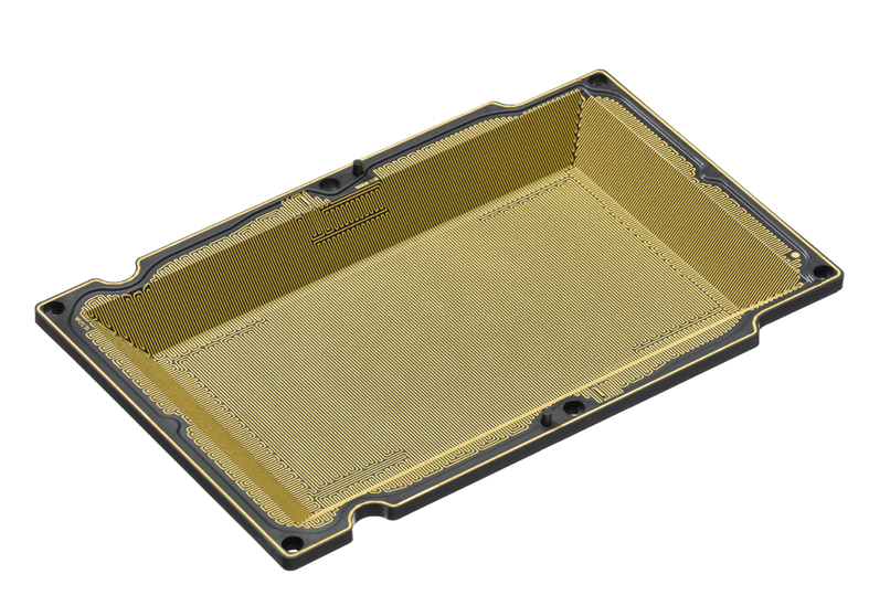 Security covers for payment terminals
The 3D-MID covers from HARTING protect the electronics both mechanically and electronically against unauthorized access. A very precise meandering structure detects any access, no matter how small, and therefore prevents theft.
More growth for 3D-MID
HARTING reports an increased demand for MID projects and has further expanded the 3D-MID division by investing in machines and by acquiring a competitor's company. Innovative own products also contribute to further growth. HARTING has developed a solution based on 3D-MID technology that replaces flexible PCBs with a component carrier. Instead of using a flex PCB, the component carrier can be directly fitted with electronic components, saving up to two-thirds of the costs.