
🔧👩💻 Buildup: The Blueprint for the Multilayer 🔍🚀
For the first Technology Thursday after the summer break, we sought a straightforward explanation of the terms ‘buildup’ or ‘stackup’.
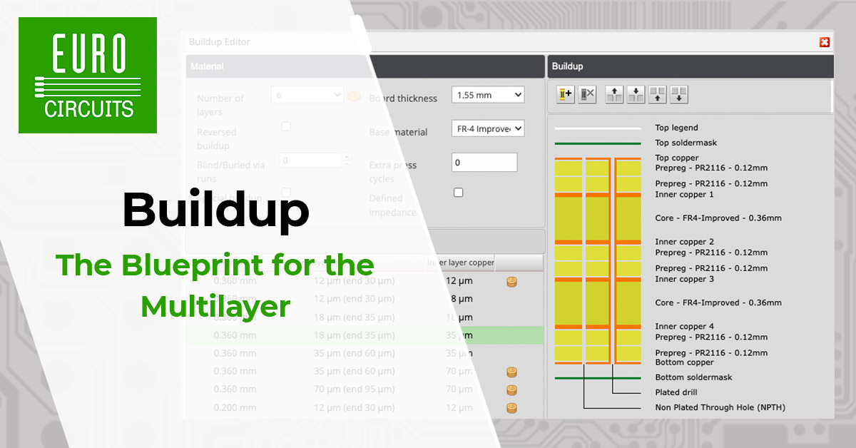
A buildup is the construction plan for a multilayer PCB and serves as the detailed description for the PCB manufacturer. It specifies the number and thickness of the copper layers, the conductive material for the upcoming pattern, and the properties and thickness of the electrically insulating layer between the copper layers, known as the dielectric.
🔍 The buildup influences mechanical stability, performance, and interference, serving as a crucial foundation for ensuring that the subsequent electronic assembly operates stably and reliably.
🔄 Due to this, the planning of the layer structure and the selection of base materials must be thorough and strategic. This process is far from trivial, as it involves numerous potential combinations of the sequence and orientation of copper layers and dielectric materials. These choices significantly impact the physical properties, manufacturability, and cost of the multilayer.
🛠️ The Eurocircuits Buildup Editor is designed to manage precisely this complexity. This freely accessible tool offers 940 predefined standard layouts, detailing the number of layers, the base materials to be used, and the required PCB thickness. The selected build up is visually displayed, and an integrated online price calculator helps you identify both the most technically suitable and cost-effective solutions for your project.
🔗 Interested in learning more? Explore the possibilities and discover how to use the freely accessible Buildup Editor here. 👇
https://www.eurocircuits.com/ec-smart-tools-user-guides/buildup-editor/
hashtageurocircuits hashtagelectronics hashtagPCB hashtagpcbdesign hashtagpcbassembly hashtagpcbmanufacturing