Tijdens het Tomorrows Electronics seminar verkennen we drie baanbrekende ontwikkelingen die de toekomst van elektronica vormgeven. Ontdek hoe fotonische chips met licht in plaats van elektronen zorgen voor snellere en energiezuinigere dataverwerking. Duik in de wereld van quantum computing, waar nieuwe rekenprincipes fundamentele doorbraken mogelijk maken. En zie hoe AI-native hardware en neuromorfe architecturen chipontwerp radicaal veranderen. Dit seminar biedt engineers, ontwikkelaars en technologiebeslissers inzicht in de innovaties die de komende tien jaar het verschil gaan maken, van fundamentele research tot industriële toepassingen. Een inspirerende vooruitblik op de volgende generatie elektronica.

Faraday | Vrijdag 25 september 10.00 – 11.30

Fotonische Chips voor Qantum Informatie Verwerking

Quantum computers kunnen fundamenteel andere problemen aanpakken dan klassieke, zogenaamde Turing-complete systemen (zoals supercomputers of smartphones). Waarom is dat zo en waarom is dat belangijk? Quantum-informatica maakt nieuwe rekenprincipes mogelijk waardoor de meeste klassieke cryptografie niet meer veilig zal zijn zodra er een voldoende goede quantum computer gebouwd is. Quantum-fotonica biedt daar een uitweg in de vorm van quantum communicatie. Recente doorbraken in optische “quantum advantage” experimenten komen aan bod. Geïntegreerde fotonische chips spelen daar een steeds grotere rol en zijn onmisbaar voor de ontwikkeling van schaalbare, universele quantum computers.


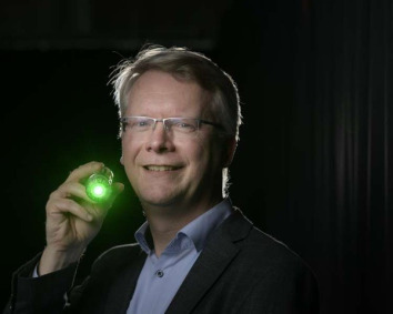
Spreker: Pepijn Pinkse, University of Twente
The Future of On-Wafer Device Characterization

The rapid evolution of semiconductor technologies—including RF and millimeter-wave electronics, advanced packaging, and quantum devices—is placing unprecedented demands on measurement accuracy, repeatability, and throughput. As device complexity increases, on-wafer characterization must evolve beyond conventional workflows that rely heavily on operator expertise toward intelligent, autonomous measurement systems.
This presentation explores how advances in metrology and automation are enabling the next generation of autonomous on-wafer measurements. Fundamental technologies for user-independent wafer probing, including automated alignment, contact verification, and measurement sequencing, will be discussed. The presentation will also demonstrate the role of traceable calibration wafers in achieving accurate, SI-traceable S-parameter measurements with quantified uncertainty, providing greater confidence in measurement results and corresponding decisions.
Building on these capabilities, the presentation will look ahead to intelligent on-wafer measurement systems that combine autonomous capability with AI-driven calibration, uncertainty estimation, and adaptive measurement strategies. Together, these developments are paving the way for faster, more reliable, and self-optimizing characterization platforms that will support future semiconductor research and industrial innovation.

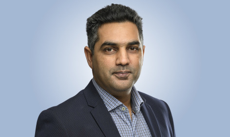
Dr. Faisal Mubarak, VSL

From lab to fab: Metrology as key enabler for quantum chips

Quantum computing has the potential to open a completely new paradigm of computing and will be one of the most important technologies of the 21st century. However, to make full impact, the number of qubits per chip needs to increase 1000x and the qubit error rates to decrease1000x, all while increasing production yield.

QuantaMap solves this by providing quantum chip metrology at cryogenic temperatures based on quantum sensing. Our NAUTILUS platform combines AFM and SQUID quantum sensors to image key chip properties, invisible to other methods, on the nanoscale. We thus enable non-invasive defect inspection and process control in the challenging operating conditions of quantum chips. This knowledge and strict process control will be critical for scaling the quantum computing industry.

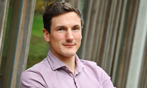
Johannes Jobst, CEO QuantaMap

FHI, federatie van technologiebranches